Products: EpiTT EpiCurve®TT SolR® News/Infos Events
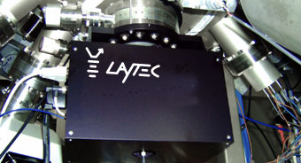
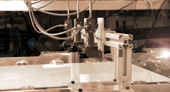
LayTec is a major provider of integrated metrology for thin-film deposition and other high value generating processes. LayTec's equipment is used in a broad range of applications like optoelectronics, electronics, PV, displays, optics and photonics, SEMI and flash memory production, automotive industry and others. LayTec's integrated metrology tools provide access to all key parameters during deposition processes in real-time - either in-situ during the process or in-line during substrate transfer between deposition chambers. LayTec's metrology is used in industry and development worldwide and offers unique benefits: process deviations are quickly identified and corrected, development cycles are accelerated, the transfer and ramp-up of established processes to new lines is facilitated and conditions are easily re-established after maintenance. In combination with LayTec's software packages for SPC (statistical process control) and APC (advanced process control), this all adds up to fab-wide optimization of processes and film quality, better production efficiency, high yields and reduced costs. In addition, LayTec metrology tools are of crucial importance in the R&D labs of research organizations where new materials, processes and device structures are developed.
copyright EpiServe GmbH 2017, all rights reserved